目錄的
-
目錄的
- Antiquitäten & Kunst
- Auto & Motorrad: Fahrzeuge
- Baby
- Bücher
- Camping & Outdoor
- Feinschmecker
- Haustierbedarf
- Heimwerken & Garten
- IT和电子
- Kleidung & Accessoires
- Modellbau
- Musik
- PC- & Videospiele
- Sammeln & Seltenes
- Spielzeug
- TV, Video, DVD
- Telekommunikation
- Uhren & Schmuck
- Wellness & Beauty
- fashion & lifestyle
- institutional food services equipment
- medical equipment, accessories & supplies
- 个人护理
- 休闲爱好
- 办公设备,用品和配件
- 商业与工业
- 家居,建筑,装修
- 家用电器
- 摩托车及配件
- 武器和弹药
- 照相机
- 花园和庭院
- 运动,娱乐及休闲
- 食物
- 高保真音響
Filters
Search
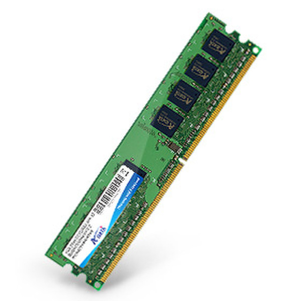
ADATA DDR2 800 DIMM 1GB 1GB DDR2 800MHz memory module
凡购买和价格 (Advertising *)
顶部
技术特点
顶部
内存参数
| 注册 | N |
|---|---|
| 内置存储器 | 1 GB |
| 内存类型 | DDR2 |
| 内存时钟速度 | 800 MHz |
| 内存格式因素 | 240-pin DIMM |
| 内存电压 | 1.8 V |
| CAS响应时间 | 5 |
| 错误更正代码 | N |
| 內存佈局(模塊 x 內存大小) | 1 x 1 GB |
DDR2 800 DIMM 1GB
A-DATA announces the Number-1 DDR2-800 module which is the first one to achieve the 800MHz of DDR2 speed in the world and pass the ATI Radeon Xpress200 QVL, and this amazing module is available now. This module configuration is by 64M x 8 (512Mbit) die, 8 pcs dies in 1 rank. DDR2-800 is officially supported by AMD AM2 and Intel x965 Platforms.
This Vitesta DDR2 module is designed to meet the 800MHz data-rate specification of the JEDEC (Joint Electron Device Engineering Council) standard, but it seems to own the huge potentiality to draw out higher performance in A-DATA laboratories.
By 1.8V low-voltage application, DDR2 modules can reduce about 50% power consumption, which is compared with 2.5V (DDR) power supply on the same operation speed. So it is an environment-friendly product. In order to achieve so amazing high operation speed, A-DATA applies the lower parasitic-loading FBGA (Fine-pitch BGA) package to run in full-speed without extraneous loading.
Compared with DDR, DDR2 owns four key technologies pave the way to high-speed operation and low power consumption.
4-bit prefectch.
DDR2 archieves the high-speed by four times the transmission amount of data . It also doubles the data rate of DDR. In the 4-bit prefetch architecture, READ or WRITE can achieve the four times the amount of data in a really internal bus clock. This is why the DDR2 can operate in four times faster than the internal operation frequency.
ODT (On Die Termination).
In DDR2, it is composed the termination resistor inside which is applied to match the transmission impedance on the mainboard. It will greatly attenuate the reflected noise resulted from last signals which improves a clear logic-level to avoid the reception of error data.
OCD (Off Chip Driver) Calibration.
OCD is the Input/Output driver resistance which applied to adjust the cross-voltage to equalize the pull-up and pull-down signal. It will greatly help to the noise-rejected quality from DDR2 module to chipset in mainboard.
Posted CAS & Additive Latency (AL).
In a posted CAS (Column Address Strobe) operation, a CAS signal (READ/WRITE command) can be input to the next clock after RAS (Row Address Strobe) signal (active command) input. The CAS command is held by the module side and executed after the additive latency (0, 1, 2, 3 and 4). It is easier controller design by avoiding collision on the command bus, and improves the command and data bus efficiency due to simple command order. It also improves the practical memory bandwidth by removing the bubble.
-
支付方式
我们接受:


