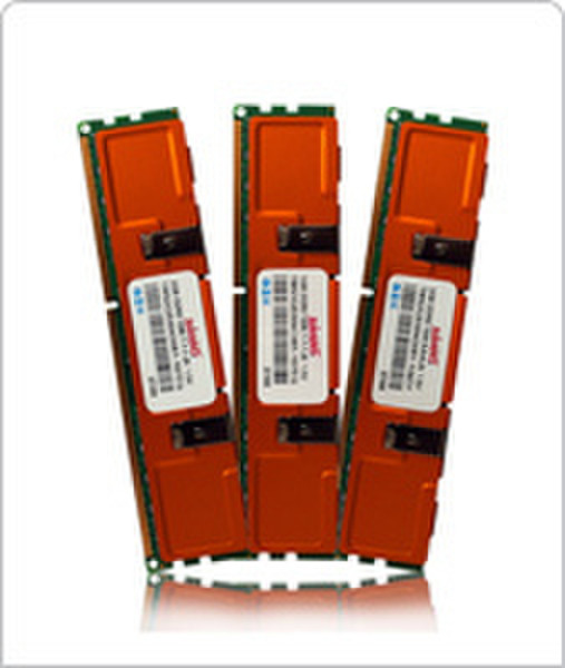
Other features
| Data transfer rate |
68224 Mbit/s |
| Power consumption (read) |
2000 mA |
| Power consumption (write) |
2000 mA |
Memory
| Internal memory |
2 GB |
| Internal memory type |
DDR3 |
| Memory clock speed |
1066 MHz |
| Memory form factor |
240-pin DIMM |
| Memory voltage |
1.5 V |
| CAS latency |
7 |
| ECC |
N |
| Memory bus |
64 bit |
| Registered |
N |
| Read speed |
8528 MB/s |
| Write speed |
8528 MB/s |
DDR3-1066 F, 2GB
These memory devices are JEDEC standard unbuffered DIMMs, based on CMOS DDR3 SDRAM technology using DDR3 SDRAMs in FBGA packages on a 240-pin glass epoxy substrate. The memory array is designed with Double Data Rate (DDR3) Synchronous DRAMs for unbuffered applications.
Fly-by command/address/control bus architecture of DDR3 SDRAMs allows
for concurrent operation, thereby providing high, effective bandwidth. This main benefit of DDR3 is made possible by its 8 bit prefetch buffer.
DDR3 memory ensures a power consumption reduction of 30% compared to
DDR2 modules due to DDR3's 1.5 V supply voltage, also defined as "Enhanced low power features".
These modules feature Serial Presence Detect (SPD) based on a serial
EEPROM device. DDR3 SPD programming is based on a speed bin. DDR3 latencies are numerically higher because the clock cycles by which they are measured are shorter. Absolute latency (ns) is generally equal to or faster than DDR2.